This page is out of date. The current page for R53 Logger - Flasher — what it costs, which ECUs it can write, and what is still beta — is R53 Logger - Flasher on the Play Store.
The CAN shift light was supposed to be a weekend job. Read RPM off the bus, light up eight LEDs, done. It has since grown a second job and then a third, and what is in the footwell now is a small bridge that does all of this at once:
- Reads the ECU over K-line. The R53’s Siemens EMS2000 speaks DS2, and the board negotiates the fast 62500-baud session itself at key-on. It ships raw block payloads over BLE, so the phone does the decoding.
- Listens to the CAN bus. RPM, throttle, coolant and road speed off the car’s own bus, plus AEMnet lambda from the wideband gauge spliced onto the same pair.
- Reads the chassis modules. Instrument cluster and the other body modules, on the second K-line, at the 9600 they insist on.
- Drives the shift light. Same eight WS2812Bs as before, still working with no phone connected and no app running.
All of it arrives at the phone as one merged stream. The board fuses the ECU blocks, the CAN channels and the lambda into a single feed over a single Bluetooth link, timestamped together, so the app is not stitching three sources into one row and hoping they line up.
It feeds R53 Logger - Flasher, which does the logging, the analysis and the flashing. This post is the hardware.
Everything here now lives in its own repo: R53_Mini_Kline_Canbus_Logger_Shiftlight.
The whole board in one picture
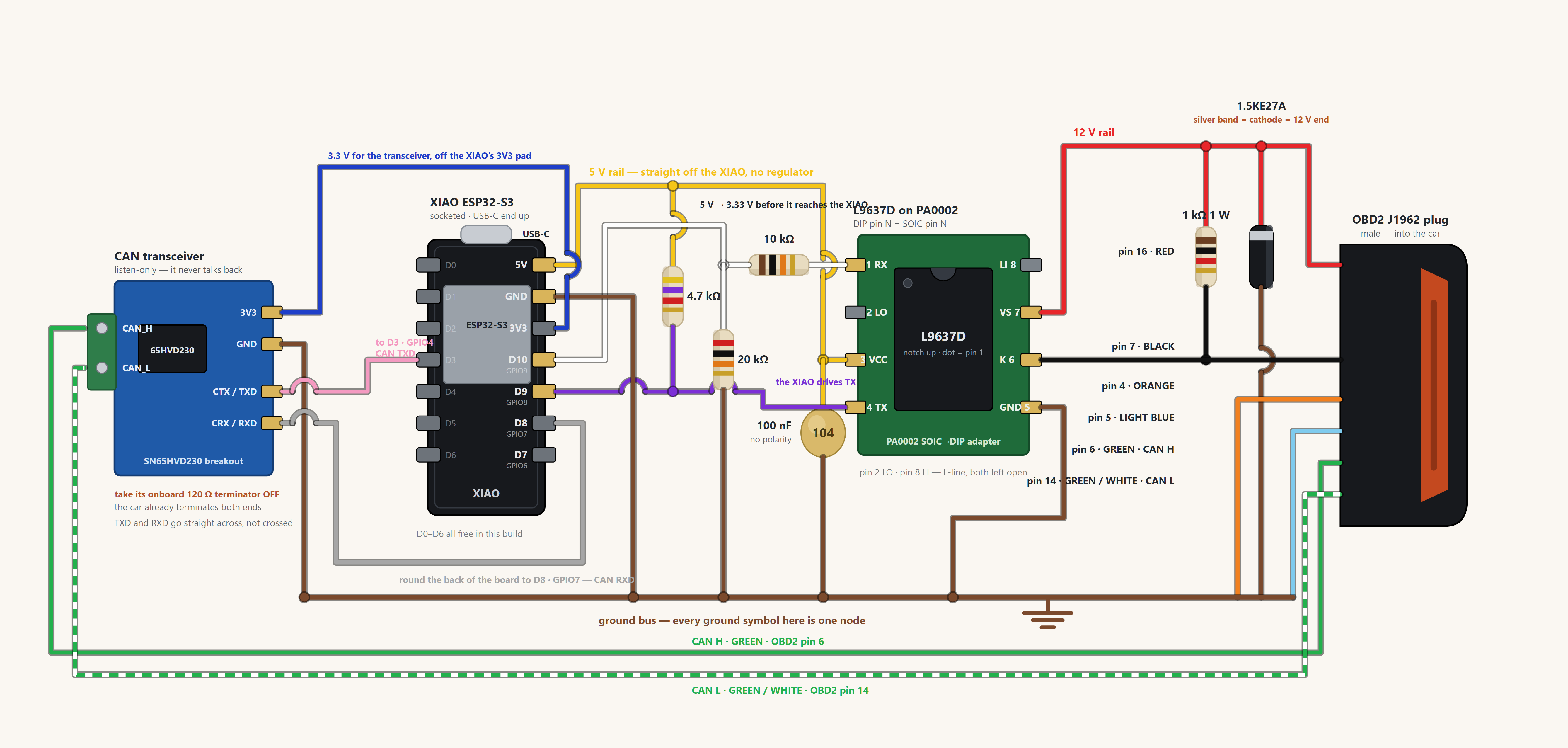
Every net gets a colour of its own, and the six car-side wires carry the actual colours of the OBD2 pigtail. Where two wires cross, the one on top is drawn with a bridge — a bridge is never a join.
The car sits on the right on purpose. The L9637D’s car-side pins (6 K, 7 VS) are on its right-hand side and its micro-side pins (1 RX, 3 VCC, 4 TX) on its left, so this is the only arrangement where no wire has to cross the chip.
The board is a XIAO, not the Waveshare
The shift light ran on a Waveshare ESP32-S3-Zero. The bridge runs on a Seeed XIAO ESP32-S3, and that swap is not free.
On the S3-Zero the silkscreen number is the GPIO number. On the XIAO it is not: D3 is GPIO4 and D8 is GPIO7. Flash the old firmware to a XIAO unchanged and the WS2812B data line comes out on GPIO4 — which is D3, the pin this wiring gives to the CAN transceiver’s TXD. The LED strip ends up driving the transceiver’s input, and the symptom is a CAN bus that appears dead.
The build config changes too. The Waveshare part is an ESP32-S3FH4R2 with 4 MB flash and 2 MB quad PSRAM, which is why platformio.ini forced a generic DevKitC with qio_qspi. The XIAO is an ESP32-S3R8: 8 MB flash, 8 MB octal PSRAM. Those overrides are actively wrong for it — and there is a real board definition, board = seeed_xiao_esp32s3, so the whole override block gets deleted rather than re-tuned.
CAN comes from OBD2 pins 6 and 14
This surprises people: the R53 does not carry the powertrain bus to the OBD2 socket from the factory. So this is not a tap. The pair is being run to the connector and landed on pin 6 (CAN H) and pin 14 (CAN L), which makes the socket the single service point for CAN, 12 V and ground.
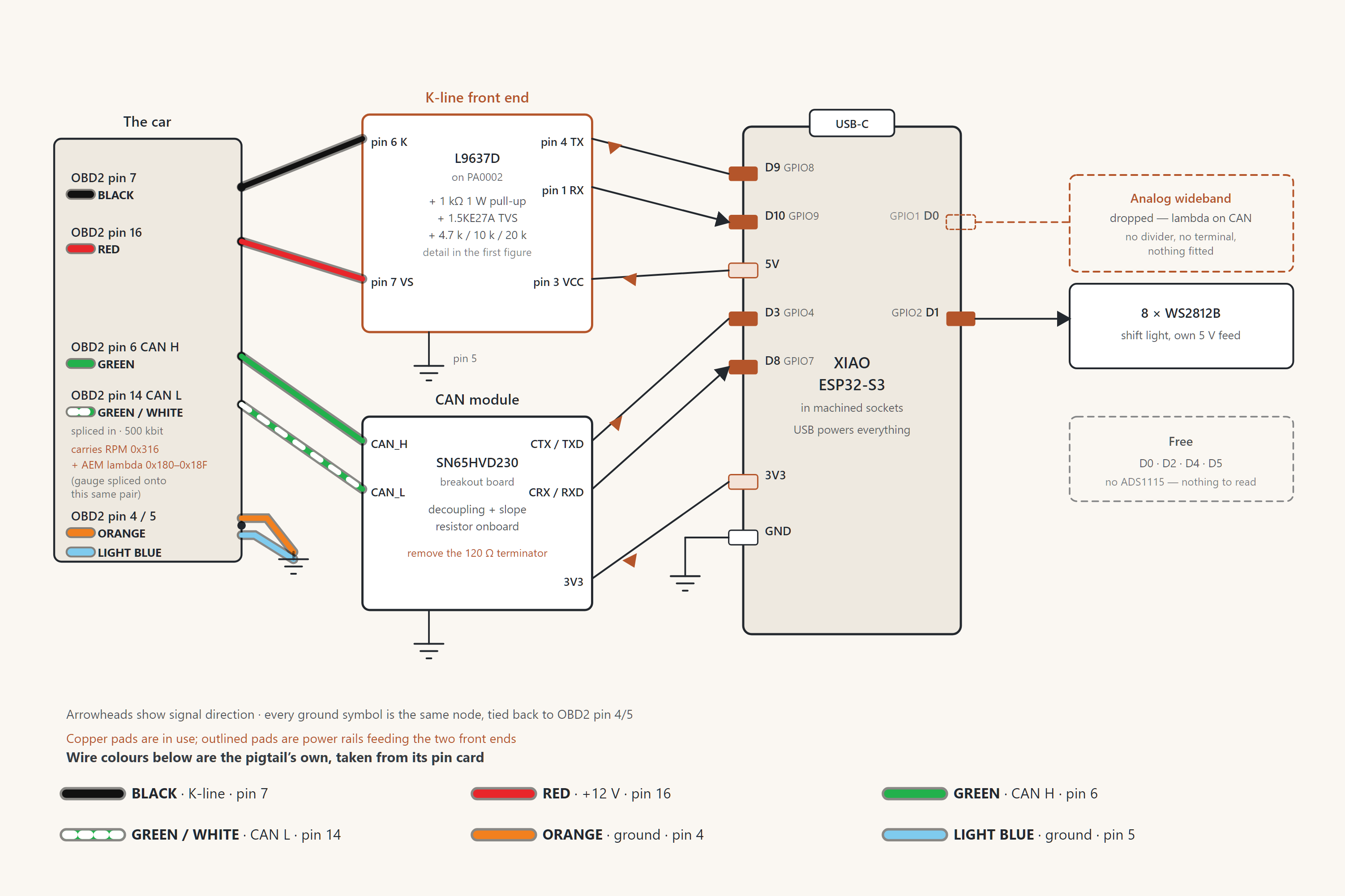
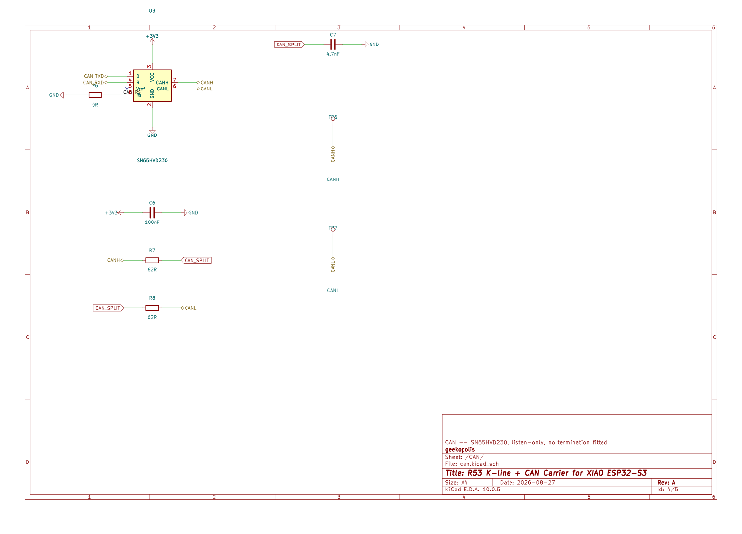
Transceiver is the usual blue-terminal SN65HVD230 breakout off the XIAO’s 3V3 pad. Two things about it:
- Take its 120 Ω terminator off. With the AEM gauge on the same pair the bus already has the car’s two ends terminated. Key off, CANH–CANL should read about 60 Ω; 40 Ω means a third terminator is still in circuit.
TXDandRXDgo straight across, not crossed. On the moduleTXDis an input the micro drives andRXDis an output. Swapping them is the classic reason a freshly built CAN node hears nothing.
The ESP32 stays in TWAI_MODE_LISTEN_ONLY, so it never ACKs and cannot disturb the bus whatever else is going on.
The K-line front end
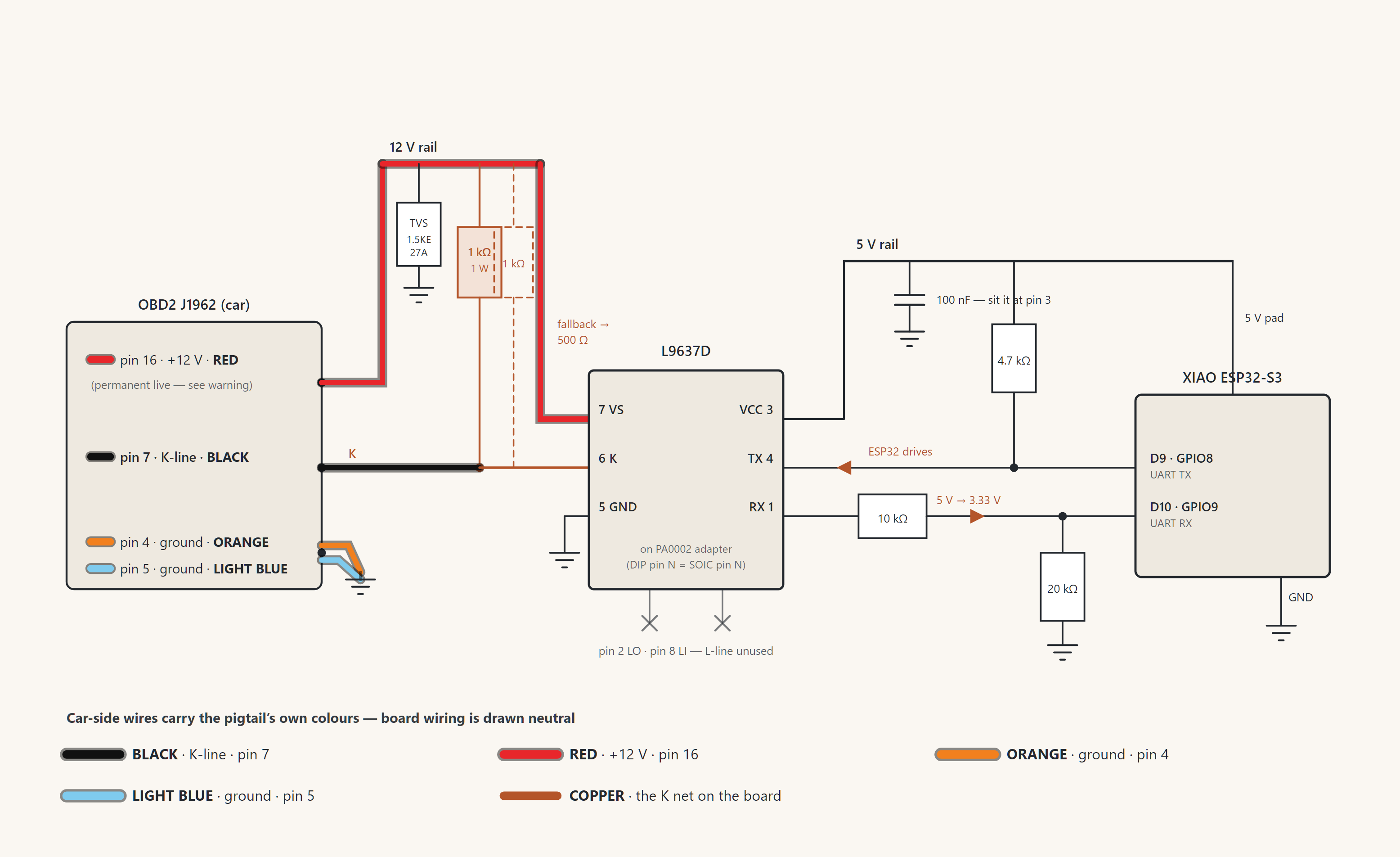
K-line is a single bidirectional wire idling at battery voltage, so it needs a real transceiver rather than a transistor and hope. This uses an ST L9637D on a PA0002 SOIC-8 → DIP-8 adapter, which is convenient because DIP pin N is SOIC pin N.
Around it:
- 1 kΩ 1 W from the 12 V rail to the K net — the pull-up that idles the bus high. One watt, not a quarter; it sits across 12 V whenever the line is pulled low.
- 1.5KE27A TVS from the 12 V rail to ground, clamping whatever the car throws at it.
- 4.7 kΩ from 5 V to the L9637D’s TX pin, which is open-drain.
- 10 k / 20 k divider on the way back, because the L9637D’s RX output swings to 5 V and the ESP32 wants 3.3 V.
- 100 nF sat right at pin 3.
The one requirement that drove the transceiver choice: 62500 baud. That is the programming-session rate, and a bridge that cannot hold it is not worth building — it would log fine and then be useless for anything else. It holds it on the car, with a single 1 kΩ pull-up, and that rate is what the whole logging and backup story below depends on.
The OBD2 pigtail, and reading it properly
The harness is a J1962 male plug on a 16-way flying-lead pigtail. Six wires used, ten cut back.
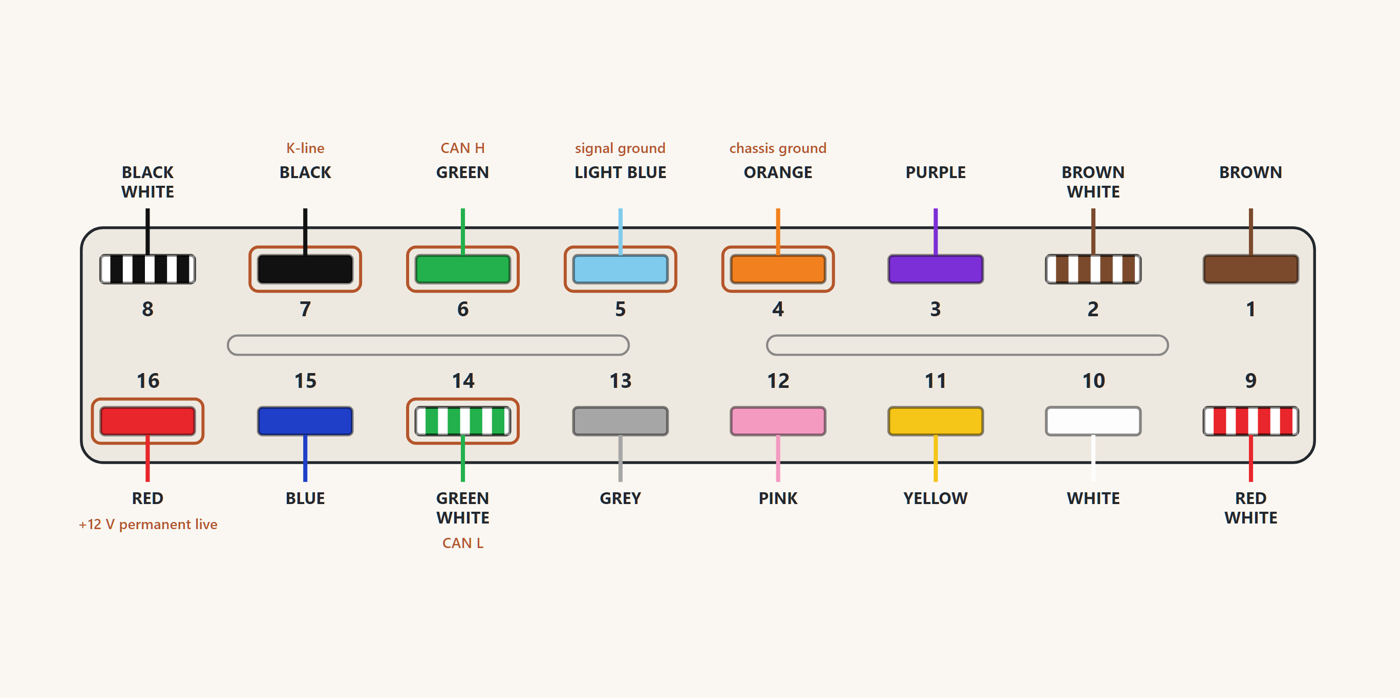
| Pin | Colour | Signal |
|---|---|---|
| 4 | Orange | chassis ground |
| 5 | Light blue | signal ground |
| 6 | Green | CAN H |
| 7 | Black | K-line |
| 14 | Green / White | CAN L |
| 16 | Red | +12 V permanent live |
Those are the colours on the card that came with this particular pigtail. J1962 standardises the pin functions and never the wire colours, so the card is the vendor’s claim about their own product, and it cannot tell you whether your cable was actually assembled to it.
Two minutes with a meter is worth it on exactly two of them:
- Pins 6 and 14. Swapping CAN H and CAN L damages nothing, but it leaves the node deaf — which looks identical to a dead bus, so you would spend an hour debugging the wrong thing.
- Pin 16. For the opposite reason: it is permanent battery, not switched, and it is not fused.
Bond both grounds to the board. Pin 4 and pin 5 are joined in the car anyway, and it gives the 12 V side a lower-impedance return.
While you are at it: cut the ten unused leads back to different lengths and heat-shrink each individually. A bundle of bare ends all cut to the same length is a short waiting to find the chassis.
Two orientations will destroy something
Everything else in the BOM fits either way round. These two do not.
The 1.5KE27A is unidirectional. Its silver band is the cathode, and that band goes to +12 V. Fitted the other way round it conducts on the first key-on and becomes a dead short across the battery. (The CA suffix is the bidirectional variant — this is not that part.)
The L9637D has a pin 1. It is marked by the dot in the corner of the package, with the notch at the same end. Get it backwards and 12 V lands on the wrong pins.
Resistors and the ceramic cap have no polarity at all, so those are free.
Where it stands — it is on the car
The board is built, flashed and running in the footwell. Every job on the list above happens at once, on one board, over one Bluetooth link.
8.5 Hz, and the phone is not in the loop
The number that matters for logging is how many complete rows per second reach the phone, and that is 8.5 Hz now, up from 3.5.
Most of that came from moving the session onto the board. The bridge probes the ECU at key-on, negotiates the 62500-baud session itself, and then runs the poll rotation on its own — the phone hands it a list of blocks once and receives a stream. Previously every single block read cost a round trip out to the phone and back before the next one could start, and on the car that round trip measured 60 ms out of every 142 ms exchange. Nearly half the sample period was spent asking permission for a request that had already been decided.
The rest came from the main loop. Each subsystem already paced itself, so the 20 ms delay holding the whole loop together was pure latency; at 1 ms nothing else changed and the rate more than doubled.
The rotation lives in the board’s flash, so it survives a reboot. Pull the bridge’s power mid-drive and it comes back on its own, re-negotiates the fast session and picks up the same list of blocks it was running before.
One stream, not three
The wideband, the CAN channels and the ECU blocks all arrive on the same link, merged on the board. That is worth more than it sounds. The lambda reading and the load and rpm it belongs with are sampled and sent together, so a fuelling number and the conditions that produced it are the same row rather than two rows that happen to be close in time.
It reads the whole ECU now
Two things that used to need the cable now work over Bluetooth:
- Chassis number from the instrument cluster, so the app knows which car it is plugged into and applies that car’s wideband calibration, AFR targets and alarms without being told.
- A full 512 KB ECU backup. Around seven minutes over the air, and the image is byte-for-byte identical to one read over the cable — verified by reading the same ECU both ways and comparing.
That second one is the useful one. A backup is the file you want before anyone touches a calibration, and until now it meant getting a laptop and a cable into the footwell.
Writing to the ECU still goes down the cable, deliberately. A dropped radio link in the middle of a flash is a different class of problem to a dropped log, and there is no good reason to take that risk when the cable is right there for the one operation that needs it.
Both K-lines
The R53 puts the ECU on one K-line and the body and chassis modules on a second. They come out of the OBD2 connector as two separate pins, 7 and 8, so a board landed on pin 7 talks to the engine and hears nothing else on the car.
Linking the two pins is the whole of it. That is what a K+DCAN cable does internally, and it is the reason one of those talks to every module rather than just the engine. The bridge has a single transceiver, so it gets the same link out at the input terminal: pin 7 and pin 8 twisted together and screwed into one position on the block. No firmware change, no second transceiver, nothing to fit.
It is deliberately not a jumper on the PCB. There it would cost a terminal position and a net, and it would have to be assembled right to work at all. At the screw clamp it is a screwdriver, and backing it off puts the two lines back to independent if I ever want that.
With the link in, the instrument cluster answers. That is where the chassis number comes from, and it is the prerequisite for coding modules over Bluetooth rather than over a cable. Wiring detail is in the hardware notes.
One porting note worth repeating
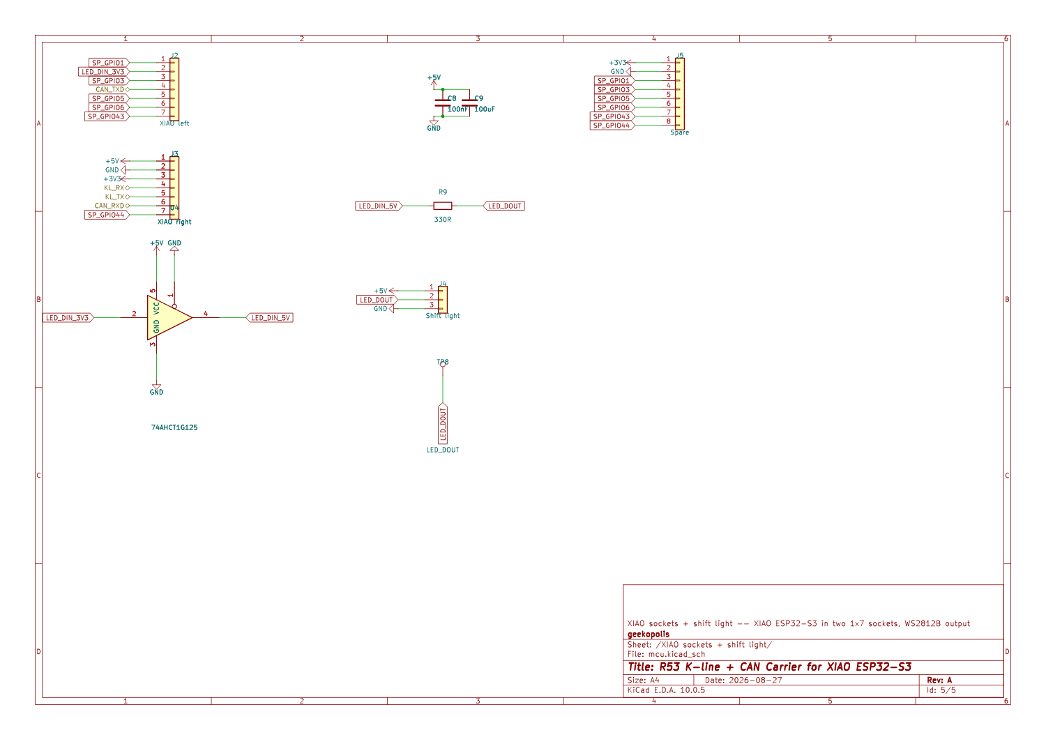
The optional ADS1115 sat on GPIO7 and GPIO8 — which on the XIAO become CAN RXD and the pins reserved for the K-line UART. The I²C bring-up is lazy, so nothing happens until the phone asks for ADS1115 mode; at that moment Wire.begin(7, 8) would seize the CAN receive line. Moving it to D4/D5 costs nothing and removes a fault that would have been miserable to find.
Full write-up of the port: PORTING.md.
It is a real board now
The wiring above describes a thing built on protoboard. It is also a PCB — 90 × 64 mm, four layers, routed clean.
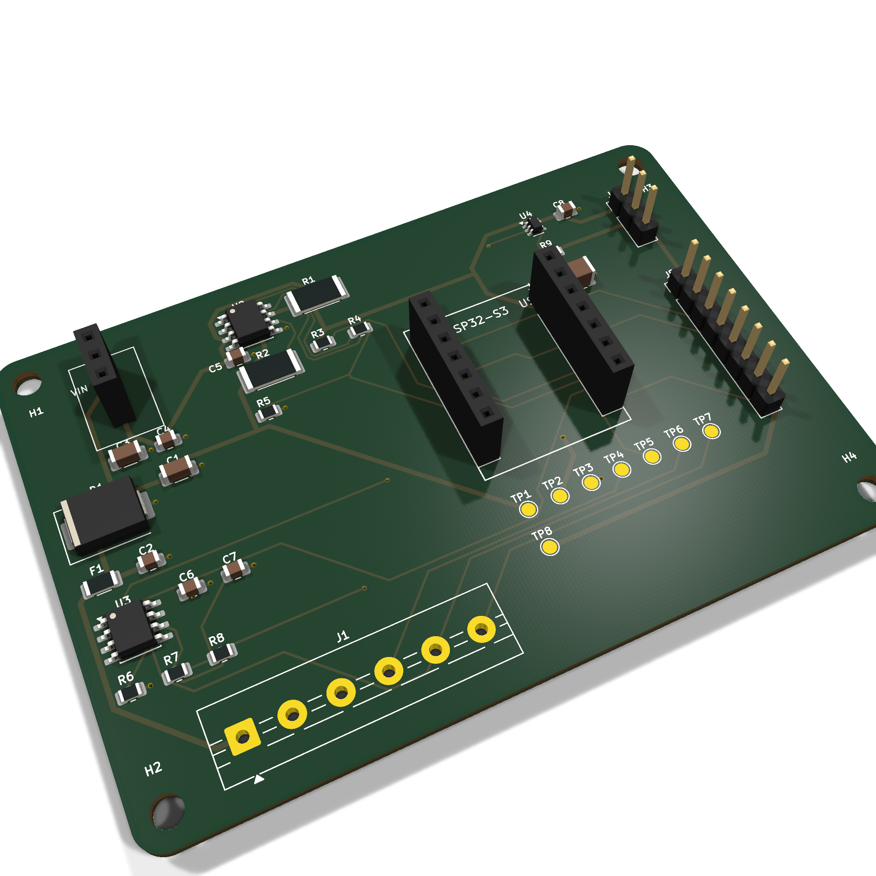
The XIAO drops into the two sockets in the middle. The car harness screws into the green block along the bottom, and the 5 V module stands in its own three-way socket top left.
Fifteen test points, all plated through-holes, differing only in size:
| count | drill | nets | |
|---|---|---|---|
| Signal | 6 | 0.7 mm | VBAT_F, K_LINE, KL_RX, CANH, CANL, LED_DOUT |
| Rail tap | 9 | 1.0 mm | 2 × 3V3, 1 × EXT_3V3, 4 × ground, 2 × 5 V |
The signal points were SMD pads first, on the reasoning that a scope tip only needs somewhere to touch. That left the board carrying two visibly different kinds of test point, and the first person to look at a photo of it read them as duplication — reasonably, because a distinction you have to explain is a distinction that is not working. A drilled point does everything the SMD pad did and takes a probe hook or a soldered wire. There was never a reason to have both, and defending the split was the wrong instinct.
The rails had a subtler version of the same problem: three taps on +3V3 — the XIAO’s own regulator, the one you should not load — and none at all on EXT_3V3, the AMS1117 rail that exists precisely so something can be hung off it. One got repointed.
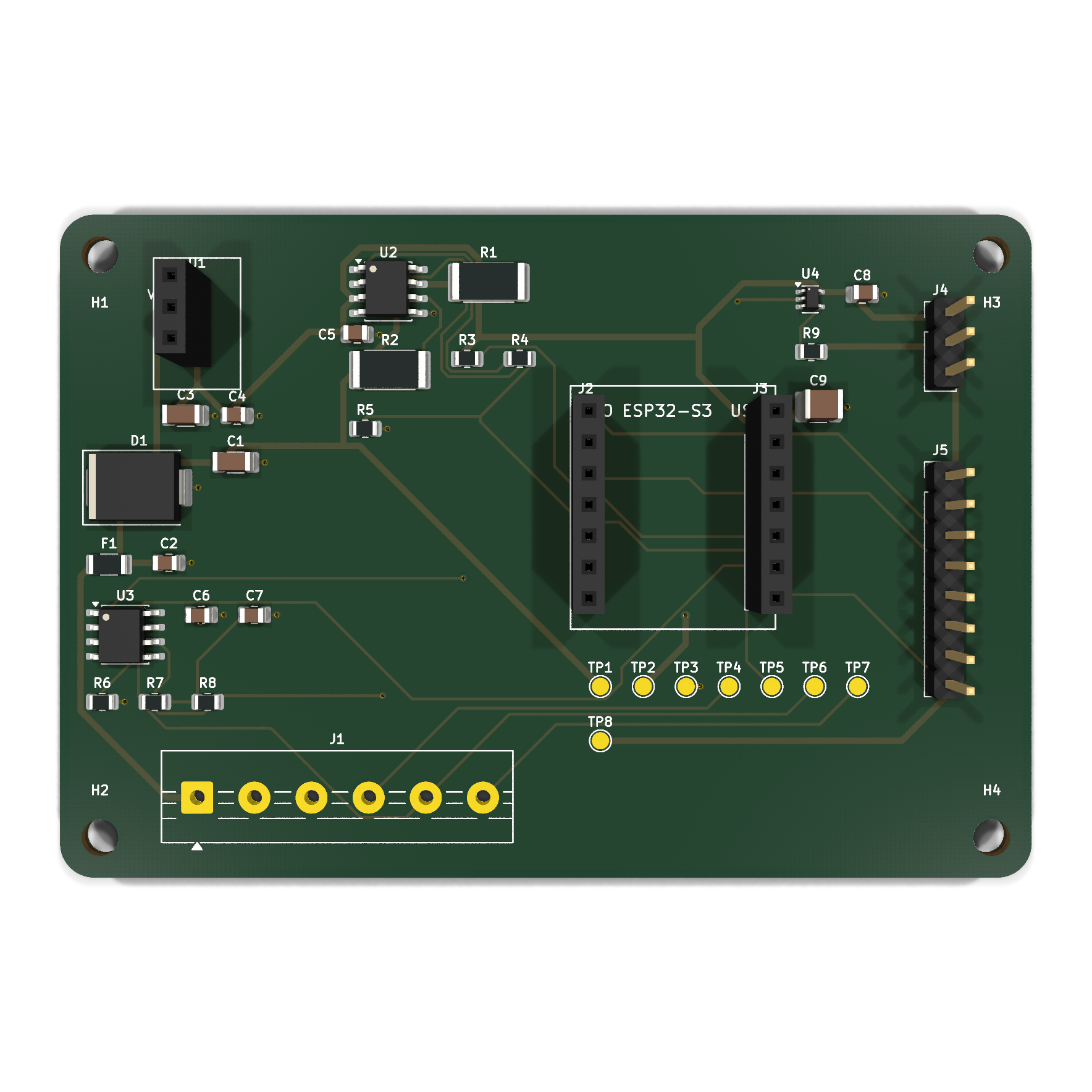
Everything surface-mount is on the top side, in packages nothing exotic — SOIC-8, SOT-353, SOT-223, SOT-23, 0805, 1206, 1210, SMA, SMC. Nothing leadless, nothing on the bottom. That started as a constraint for reflowing it on a hotplate and turned out to be the right shape for machine assembly too.
The through-hole parts are deliberately not on the assembly BOM: the two XIAO sockets, the screw terminal, the microSD socket, the spare header, the shift-light header and the 5 V module’s socket are a handful of easy hand-solder joints on a board that arrives otherwise finished.
The schematic
Four sheets. The netlist is written in Python and the KiCad files are build outputs — python gen/build_board.py places, routes, stitches the planes and tidies the silkscreen from nothing.
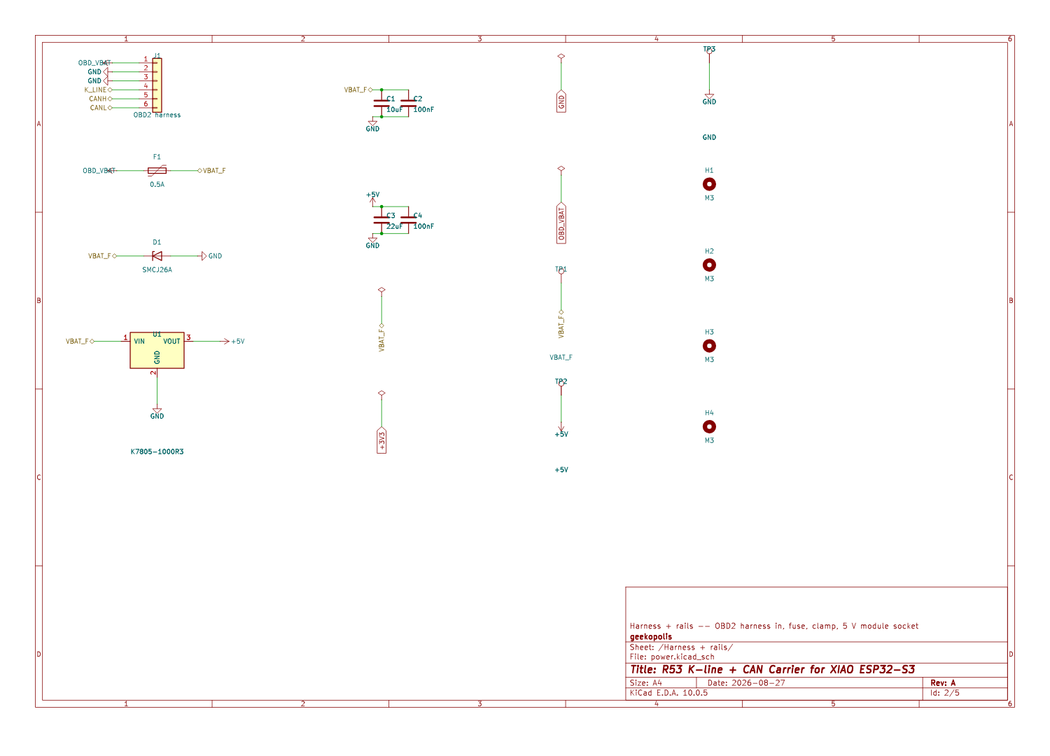
Fuse, then clamp, then module, in that order. Pin 16 is permanent live and the car does not fuse it, so the polyfuse is there to stop the OBD2 wire becoming the fusible link no matter what the TVS decides to do.
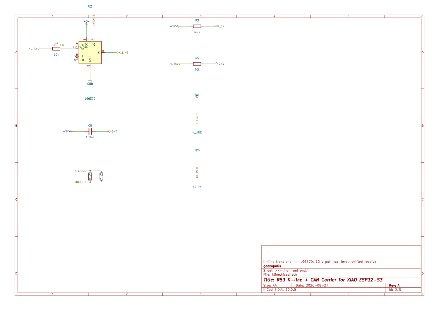
Note the two 1 kΩ pull-up positions in parallel. The second is not fitted. If 62500 baud will not frame cleanly the fix is a stiffer pull-up, and 500 Ω should cost a soldering iron rather than a board respin.
It is 12 V automotive, which is not the same as 12 V
Two things were missing and both are the kind that only bite once.
Reverse polarity. The harness lands on a screw terminal. Red and black are one slip apart, in a footwell, probably in the dark — and the only thing between that and the switching module was a polyfuse, which is a thermal device that takes seconds. There is now an SS34 Schottky between the fuse and the clamp, so reverse voltage never reaches the TVS and a backwards harness is simply an open circuit rather than a short. It costs 0.4 V against four volts of headroom.
The CAN pair had no clamp at all. CANH and CANL leave the box and run the length of the car. One PESD1CAN — two TVS sharing a middle ground pin — covers both lines in a single SOT-23.
One thing I have left as a known limitation rather than pretend away: the module needs 8 V in, and cranking pulls a tired battery below that. The board will reset on every start. Not damage, but you lose the log across exactly the moment you might want it, and fixing it properly means a buck-boost rather than a buck.
Six spare pins did not fit three ideas, so one of them moved onto the board
The original plan was an expansion header carrying the six XIAO pins the board does not use, and three things to eventually hang off it. The arithmetic never worked:
| bus | pins | |
|---|---|---|
| microSD | SPI | 4 |
| GPS | UART | 2 |
| 9-axis IMU | I²C | 2 |
| wanted | 8 | |
| available | 6 |
An SD card and a UART GPS cannot coexist on six pins. Rather than leave that as a decision for later, the microSD won and is now on the board — a 1×6 socket that takes the standard Amazon breakout directly, in the pin order printed on the module: 3V3 / CS / MOSI / CLK / MISO / GND. It takes the SPI bus, and what is left over is the I²C pair, on a smaller spare header.
So the header is now six ways of 5V / 3V3 / GND / GND / D4 / D5 — both rails and the I²C pair, which is an IMU, or an I²C GPS, or both sharing the bus.
The AMS1117-3.3 is now fitted, not a footprint. The XIAO’s own regulator is already carrying the ESP32-S3 and the CAN transceiver, and a card mid-write on top of a WiFi burst is asking too much of it, so the card gets its own 3.3 V from the 5 V rail.
That regulator is the one part on this board whose heat is a decision rather than a rounding error. It is linear, dropping 1.7 V, so every milliamp the card draws becomes heat in a SOT-223:
| sustained | dissipated | rise |
|---|---|---|
| 100 mA | 0.17 W | ~13 °C |
| 200 mA | 0.35 W | ~26 °C — a card in SPI mode |
| 500 mA | 0.85 W | ~65 °C — too hot in a car |
Roughly 300 mA of headroom, which is fine for a card and not fine for a card plus something hungry. Anything added later goes on its own regulator, or takes 5 V and makes its own.
The socket footprint was guessed, then built backwards
J5 started as a stock PinSocket_1x06 — which is exactly the mistake the 5 V module footprint made earlier in this project and was supposed to have taught me not to repeat. A stock socket footprint describes the socket. The thing that occupies the space is the module standing in it, and nothing checked whether that module actually fit.
I guessed 15 × 15 mm. A photo of the real part, ruler included, said otherwise:
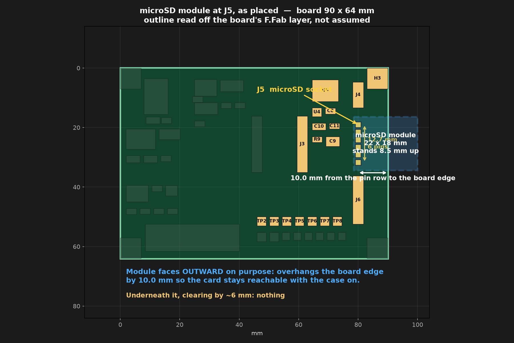
18 × 18 mm PCB, 20 mm across including the folded-steel card-slot shell. Building the footprint against that number instead of the guess, I turned the module to face inward, over the board, reasoning that facing outward it would hang most of its length off the 10 mm of clear board past J5. Facing inward it collided with four other parts the moment the real size replaced the guess — but the collision was the second problem, not the first. The first is that a microSD slot facing into the board interior is not reachable. You cannot remove a card you cannot get a finger on.
The fix was to face it outward, the way J5 was placed to begin with, and let it overhang the board edge — on purpose. The enclosure gets a cutout above it, so the card comes out without opening the case:
Ten millimetres of unsupported PCB, held only by the six-pin header. That reads as a defect in isolation and is a requirement in context — it is the reason J5 sits this close to the board edge at all. The lesson is not “measure the part,” although that’s true too. It’s that a fix which makes the geometry work can still be backwards, if the reason the geometry was wrong in the first place was that something has to be reachable by a human hand.
Two things the tooling caught that I would have missed
The TVS is drawn as a Zener. KiCad has no unidirectional-TVS symbol, and Device:D_TVS is the bidirectional one — which reads identically either way round. This part does not: reversed, it is a forward diode across the battery and it conducts on the first key-on. Drawing it with a cathode means the polarity audit can check it, and it does.
The 5 V module’s footprint was wrong by the size of the component. U1 is a socket, and a stock PinSocket_1x03 footprint describes the socket — 3.6 × 8.7 mm. The thing that actually occupies that space is the module standing on it, 11.5 × 7.6. So DRC was happy to let five parts sit underneath the module, and said nothing, because it is a 3D clearance against a part that is not on the board. The footprint now carries the module’s body as its courtyard, which turns “remember this” into a check the board makes every time it is rebuilt.
Where the XIAO’s dimensions came from
The socket row spacing is not in any spec table Seeed publish. It came out of their own KiCad PCB file for the part, opened with pcbnew and asked for its through-hole pads:
column x =  1.260   7 pads, 2.54 mm pitch   (pins 1-7)
column x = 16.500   7 pads, 2.54 mm pitch   (pins 8-14)

ROW SPACING = 15.240 mm, exactly 0.600"
The two further columns in that file, at x = −0.010 and x = 17.770, are the castellated half-holes on the board edges. A footprint built from those would be 2.5 mm too wide, and would look perfectly reasonable right up until the module would not go in.
The same file answered the antenna question. ANT1 on a XIAO is a U.FL connector, not a PCB antenna — so the module radiates from a pigtail, copper underneath detunes nothing, and the ground plane stays whole under the CAN pair, which is where it is actually wanted.
The assembly BOM was wrong in both directions
This one is worth the warning. The fab files were generated by a script forked from an earlier board, and that script carried a hardcoded list of parts to leave off — {"C3", "C6", "C7"}. Those are reference designators. On the earlier board they were aluminium electrolytics the assembler could not source. On this board C3 is the 5 V module’s output bulk and C6 is the CAN transceiver’s bypass.
Carried over unread, it silently dropped two capacitors that must be fitted. The boards would have arrived built, looking entirely correct.
It was also including three parts the design says to leave off: a second 1 kΩ that would have made the K-line pull-up 500 Ω, and two 62 Ω that would have put ~124 Ω across a CAN bus the car already terminates at both ends. That board would have come back measuring 40 Ω where the documentation says expect 60, and nothing would have looked wrong.
Both directions are now driven off the netlist note rather than a designator list, so it cannot rot the same way. The lesson generalises: a hardcoded list of reference designators is a landmine in any file you fork.
Five failures that printed reassuring output
That BOM bug turned out not to be the only one of its shape, and the rest surfaced in a single evening of checking the board before ordering it. Every one of them produced plausible, confident output while being wrong. None produced an error.
A comment made every power rail thin. The note explaining why the Power netclass is 0.60 mm was written inside the JSON template that generates the KiCad project file. That made the file unparseable, so KiCad silently reset the net settings to a single default class and routed every rail at 0.25 mm. Nothing failed, because narrow track is legal track. The only symptom was an ampacity note in my own audit, which for a while I read as a routing problem.
Two rails had no netclass at all. VBAT_FUSED — the far side of the reverse-polarity diode, carrying identical current to VBAT_F — and the new LDO output. A rail that gets renamed halfway through a schematic needs a glob, not a second entry someone has to remember to add.
Three audit tables were describing a different board. They were forked from an earlier design, and named nets and parts that do not exist here: seven rails reported as “plane-fed” that were simply absent, a dissipation check pointed at two parts not on the board, and a purchasing list that called the microSD socket a spare header and omitted the actual spare header entirely. Ordering from that list would have got an unusable 1×8 and no socket for the card. All three now cross-check themselves against the generated netlist and fail loudly.
Mounting holes 0.5 mm out of square. The right-hand pair sat closer to the edge than the left, left over from an earlier outline. No copper was at risk — but anyone drilling a bracket from the pattern would have found out the hard way.
And a schematic that plotted five dead pins. This one is my favourite, because it is so specific. The function that defines a part takes (mpn, note, nc, lcsc). I passed a part number positionally in the wrong slot, so it landed in note — and the note sentence landed in nc, the list of no-connect pins. nc is iterated for pin numbers, and iterating a string in Python yields characters. Every pin whose digit appeared anywhere in that sentence got a no-connect flag. The microSD socket plotted with pins 2–6 dead.
ERC passed, because drawing a no-connect is a legal thing to do. The board was never affected, because the netlist is built from a different field — the gerbers were correct the whole time. It was caught only because I rendered the sheet and looked at it before publishing it here.
The through-line: every one of these failed by printing something reassuring. A check that examines nothing looks exactly like a check that passes. That is the case worth engineering against — not the crash, which tells you where it is.
Board files, gerbers and a BOM where every line carries an in-stock LCSC part number: hardware/pcb. Not manufactured yet — boards are on order.
Repo, with the full interactive wiring reference and every diagram above: github.com/MrBlahhhh/R53_Mini_Kline_Canbus_Logger_Shiftlight